
Applicable Targets
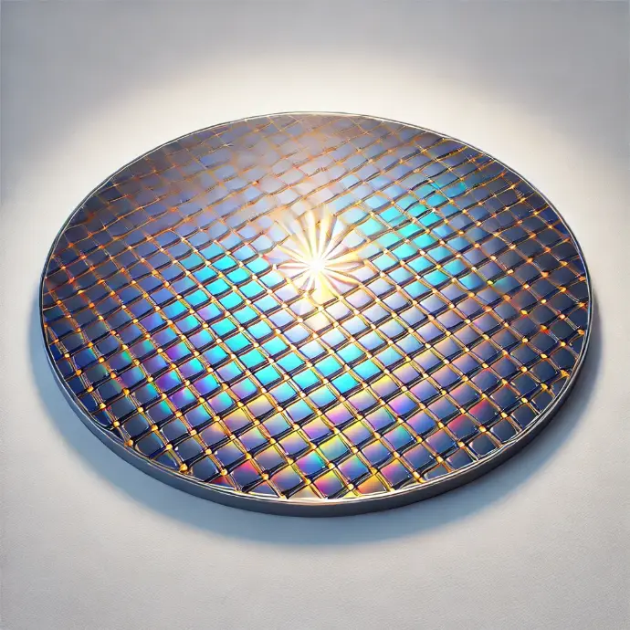
- 4/6/8/12-inch wafers
- Silicon, GaN, compound semiconductor, and glass substrates
- Wafer front side, back side, edge, and bare wafers
Fastmicro
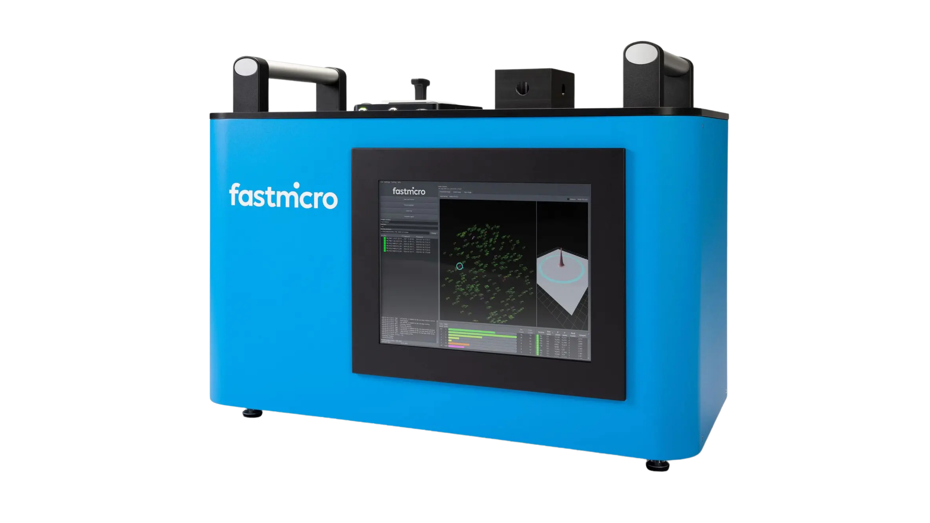
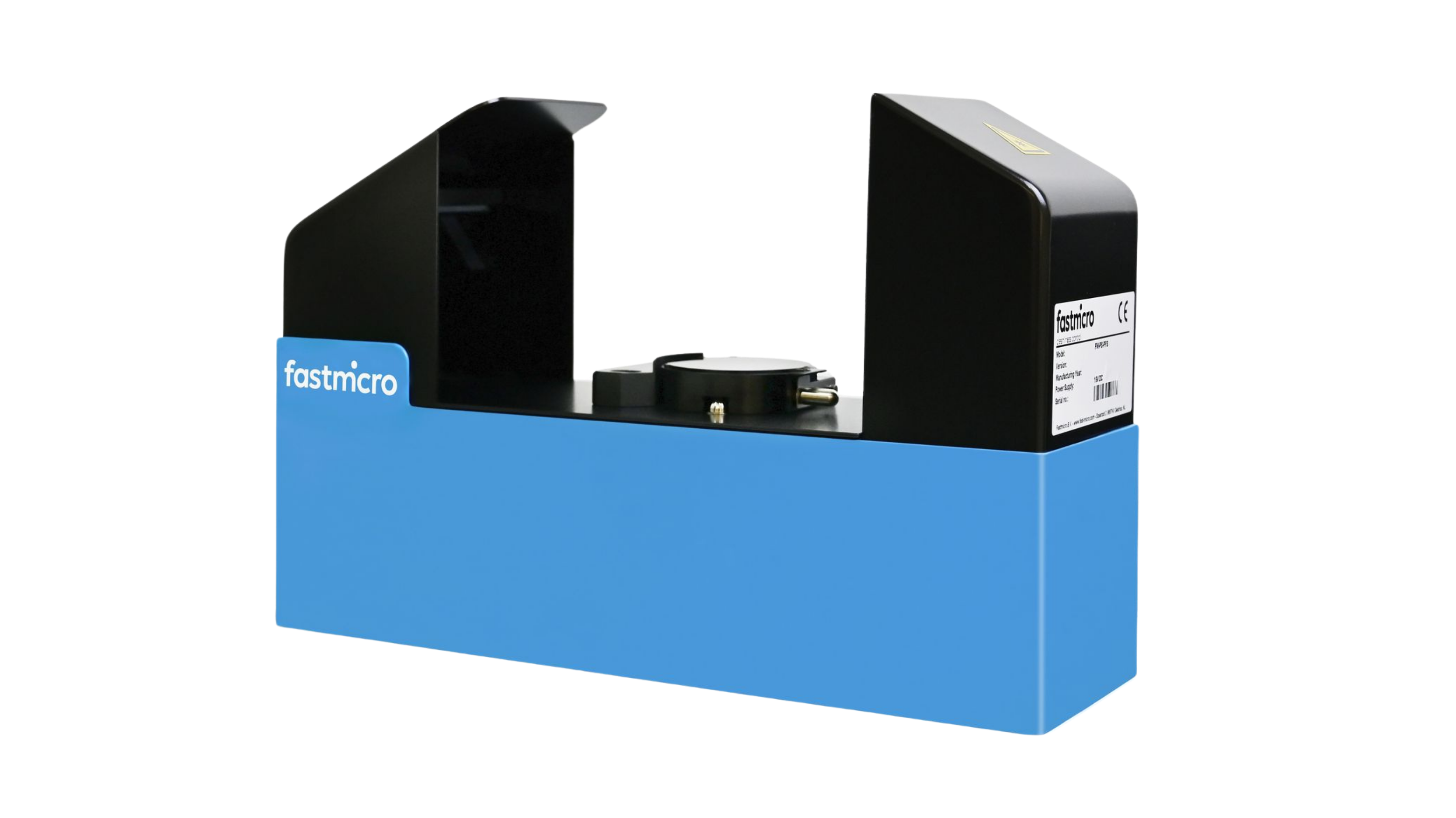
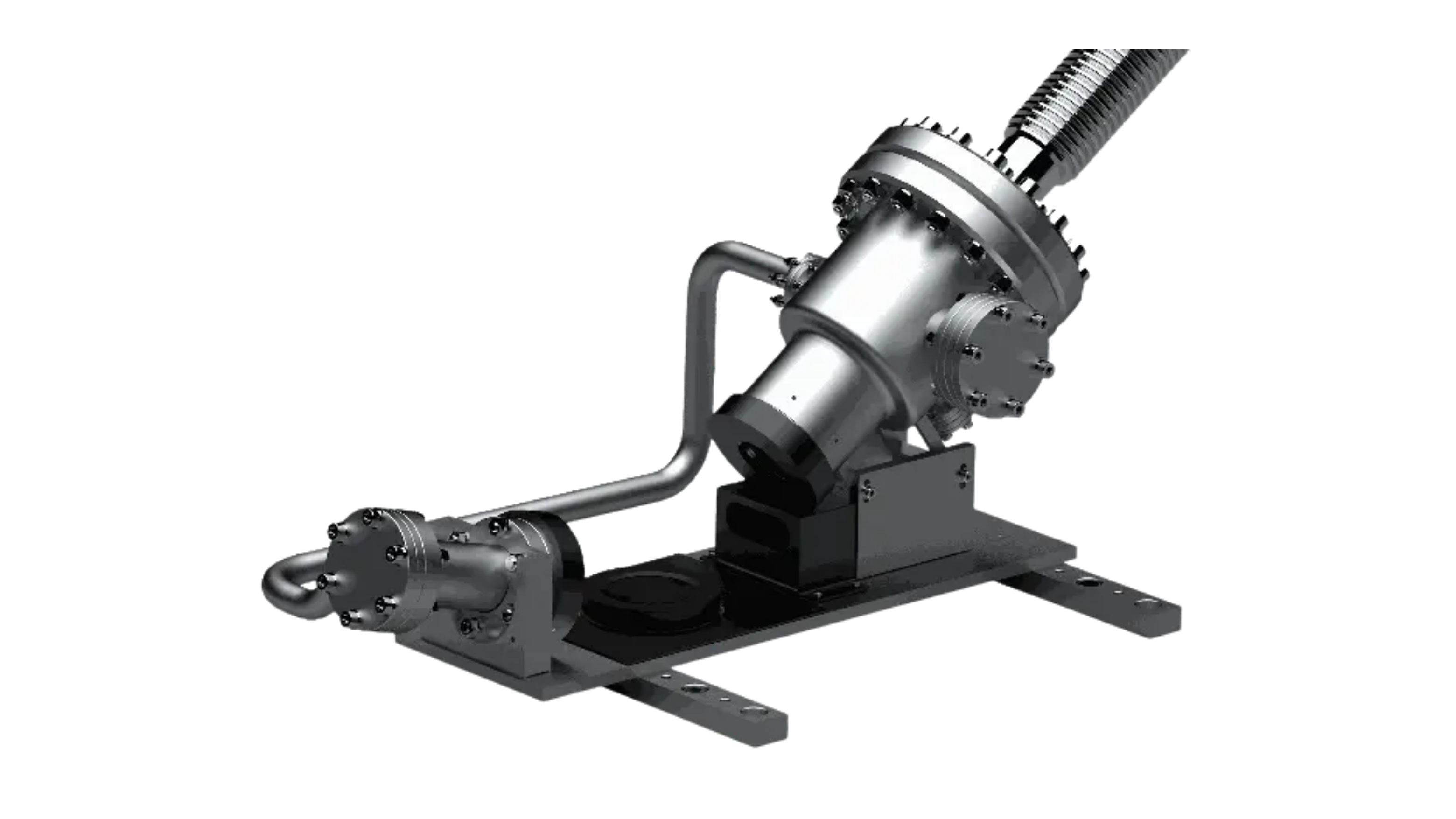
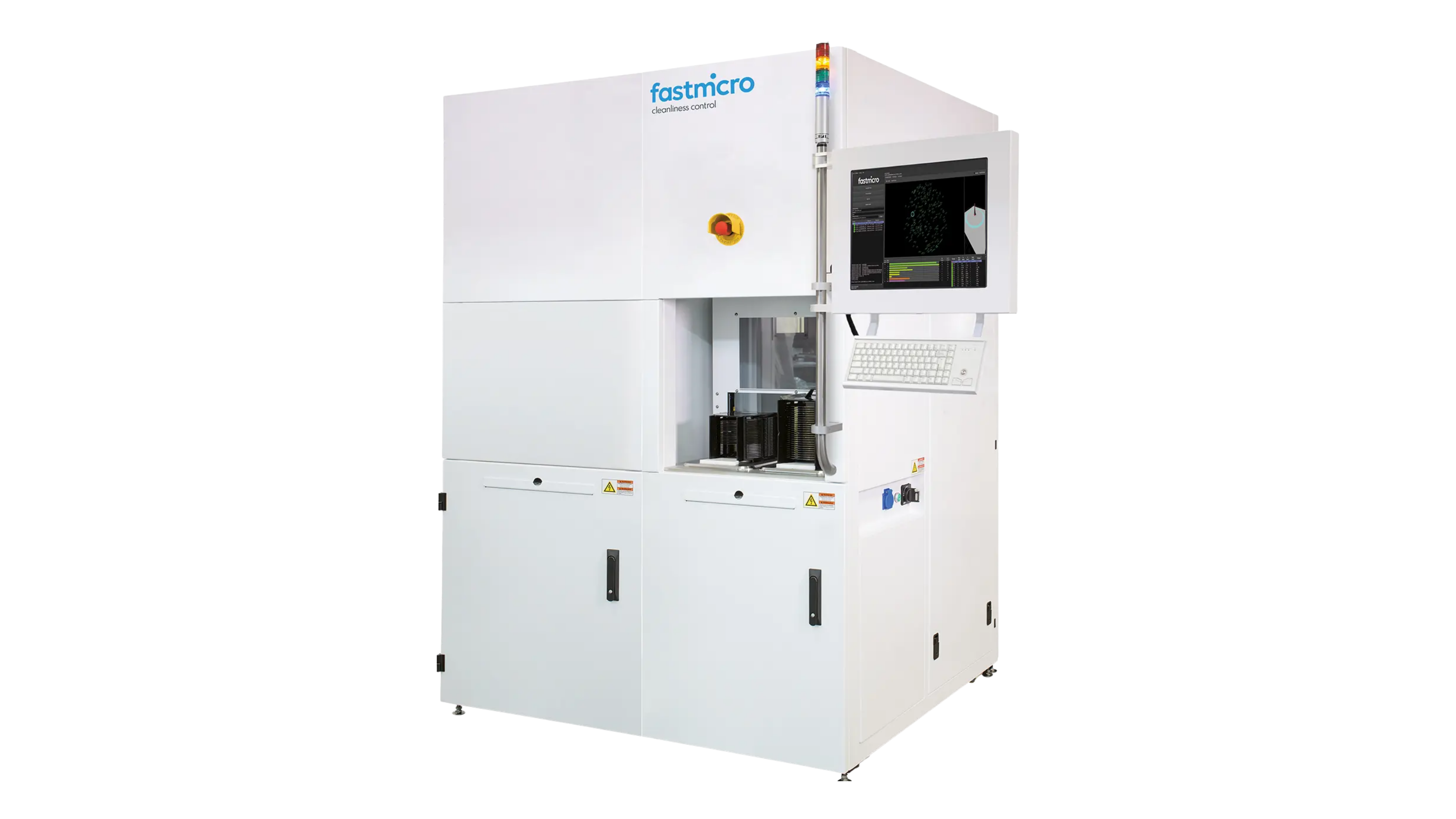
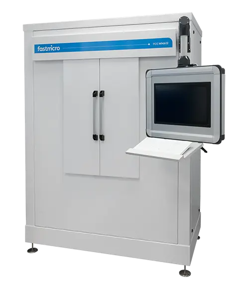
High-throughput direct surface particle and defect inspection for 4/6/8/12-inch wafers
Suitable for incoming wafer inspection, in-process monitoring, post-cleaning verification, and defect location analysis. The system provides particle count, size, and position data for process, quality, and equipment teams, enabling faster identification of contamination risks and supporting downstream analysis workflows.
PRODUCT OVERVIEW
TYPICAL APPLICATION
CUSTOMER STORY
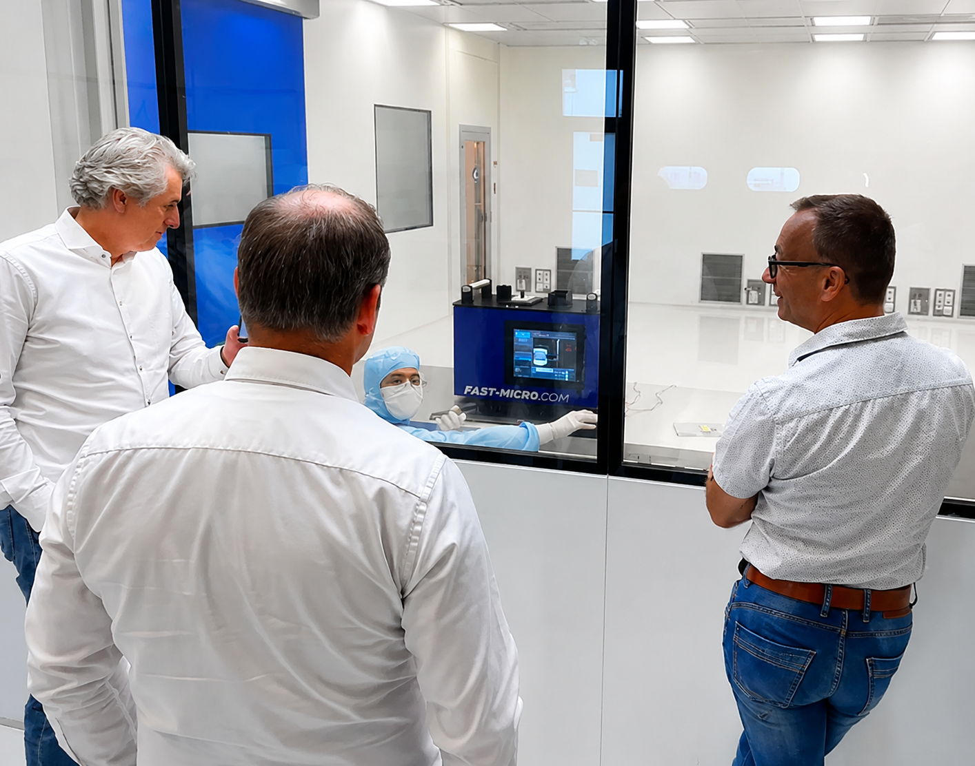
Dr. Ir. L.H.A. Leunissen | ASML, cleanliness project manager remarked: "As a long-term partner, Fastmicro's integrated application has enabled us to meet equipment defect rate targets. The system not only delivers precise measurements but is also characterized by ease of operation and high throughput. We highly recognize Fastmicro's professional service and look forward to further expanding the system's functional boundaries through deeper collaboration."
PRODUCT PARAMETER
| General Specifications | |
|---|---|
| Detection Range | From 0.1 µm PSL equivalent particles |
| Throughput | Up to 400 wafers/hour |
| Position Accuracy | 40 µm |
| Position Repeatability | 15 µm |
| Supported Wafer Sizes | 4 - 12 inch |
| Detection Capability | Supports front and back side wafer inspection applications |
DOWNLOAD CENTER
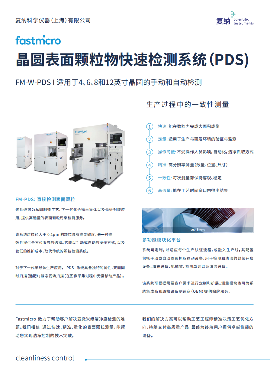
Rapid particle detection system for wafer surface contamination monitoring in semiconductor fabs.
DownloadTo learn more about our products, please fill in the form below to download the product brochure. We will get back to you as soon as we receive your information.